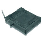
BGA Socket Information
MATERIAL SPECIFICATIONS:
Contacts
| Material |
S.S |
| Standard Plating |
30 n/PdNi |
| Optional |
30 n/NiB
30 n/Au |
| Temperature Rating |
300 |
Solder Tail Section
| Pitch 1.0, 1.27, 1.5 |
0.36 mm x 0.13mm |
| Pitch 0.80 |
0.20mm x 0.13mm |
| Solder Tail Length |
27mm Base = 3.86mm |
| Solder Tail Length |
43mm Base = 3.30mm |
| Solder Tail Length |
50mm Base = 3.43mm |
Plastic Parts
| Material |
40% Glass-Filled PPS |
| Temperature Rating |
175 Continuous |
| Insulation Resistance |
1x10¹³ Ohms/Mil |
Mounting Hardware, Cam Handle, Spring
| Material |
S.S |
| Temperature Rating |
300 Continuous |
ELECTRICAL TESTS
| Resistance (Ambient)* |
< 25 MilliOhms |
| Resistance (160癈) |
50 MilliOhms (Max) |
| Capacitance |
0.234 pF (1Mhz) |
| Inductance |
4 nH |
| Frequency Response |
Avg. Insertion Loss At 500 Mhz
Is -0.52dB |
| * HP 4328 A Milliohmmeter |
VIBRATION
| Equipment |
Fluke Data Bucket
Techtronix Oscilloscope |
| Procedure |
40 Random Contacts
Daisy-Chained Biased At 10 Volts |
| Test |
5 Cycles In X,Y,Z Axis
Linear Sweep 10-500 Hz
1 Minute Up - 1 Down
.050" Displacement, 10-53 Hz
Continuing at 10G, 53-500 Hz |
| Results |
^Resistance Was Negligible |
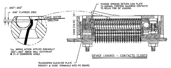
NORMAL FORCE
- 44 - 48 Grams With 0.03mm - 0.05mm Wipe
LIFE CYCLING
- Life To Be Expected: 5,000 Cycles plus
SOLDER BALL DEFORMATION
- Through a patented contact method, no scratching or deforming will occur on the reflow portion of the solder ball.
- Testing for 240+ hours at 125癈 has shown minimal impressions of 0.03mm to 0.08mm at point of contact.
Installation of Cam Handle BGA Socket onto
Burn-in Board or Printed Circuit Boar
INSTALLATION OF BGA SOCKET TO BIB OR PCB
STEP ONE
If Black Contact Protector / PCB Guide Plate on bottomside of the socket is not extended, gently pull it down or firmly tap socket on flat surface until the guide plate is flush with the bottom of the contact tails. Avoid touching the grid area of the socket while extending the PCB guide plate flush with the contact tails.
STEP TWO
Insert the locating pins on the Black Contact Protector/PCB Guide Plate into their matching holes on the PCB.
STEP THREE
Gently and evenly press down on the socket until it is seated on the BIB or PCB.
STEP FOUR
Locate the four socket screws on the backside of the BIB or PCB.Use the mounting hardware, consisting of four (4) Nylatron washers, four (4) flat washers, four (4) lock washers, and four (4) hex nuts, in that order, to secure the socket to the PCB or BIB. It is important that the Nylatron washer is mounted next to the PCB or BIB.
STEP FIVE
Gently tighten the hex nut until the split lock washers are compressed. However, if the split lock washers are difficult to see, one to two (1-2) inch/lbs of torque will be sufficient. Be cautious not to overtighten the hex nuts or damage to the BIB or PCB may occur.
STEP SIX
Rotate the cam handle or rocker cam to the open position before soldering contacts.
STEP SEVEN
Solder.
STEP EIGHT
Remove labels from the top of the socket.
LOADING THE PACKAGE INTO SOCKET
STEP ONE
Rotate the cam handle or rocker arm to the open position. If the contacts are not open when loading, damage will occur to the tips of the contacts. The rocker arm closest to the end of the socket should be down, or the cam handle vertical.
STEP TWO
Place the package with the correct predetermined orientation into the socket. Confirm that the package is properly seated by gently pressing on all four corners of the package.
STEP THREE
Rotate the cam handle or rocker arm to the closed position. Do not apply any pressure to the top of the package while closing the contacts. If pressure is applied, it is possible solder mask will be scraped onto the contact, causing an insulation barrier at the solder ball. If this does occur, clean the contacts with a vacuum brush.
UNLOADING THE PACKAGE
STEP ONE
Rotate the cam handle or rocker arm to the open position. The cam handle should be in a vertical position and very little force is needed to rotate the cam handle. Over extension could break the camming mechanism, so do not force the cam past the vertical stopping position. The rocker arm will naturally stop at the surface of the BIB or PCB.
STEP TWO
Unload the package using vertical force.
PREVENTIVE MAINTENANCE
Depending on frequency of use and the burn-in environment, the sockets should be inspected for accumulation of debris or solder material on the contacts or in the cavities. On regular intervals the socket should be vacuum brushed to remove these materials.
In addition, the contacts might be contaminated or bent if touched by human fingers. Care should be exercised during operation, storage, and inspection to prevent any contact.
For removal of solder accumulation or tin/lead on the contact tips, a citric acid wash solution can be used and will not harm the socket or contacts.
OTHER ISSUES
Opens during testing: Remove the package and do one of the following:
- Vacuum brush the contacts and socket.
- Inspect the socket contacts to see if any are bent or contaminated.
- Replace the package without pressing down on the package when actuating the cam lever or rocker arm.
REMOVAL OF PACKAGE GUIDE PLATES
The sockets have snap-on guide plates on the top surface that are fitted to the size of the specific BGA package. Attempting to remove these could result in their breaking. If for any reason removal of these plates is necessary, e.g. to allow a test gauge to fit, please call Plastronics at 1-800-582-5822 for instructions. If the guide plates do break, do not replace them into the socket. Call Plastronics for replacements or instructions. |